- Nvidia invested $2 billion in Marvell Technology — opening its proprietary NVLink interconnect to third-party silicon for the first time through the NVLink Fusion platform
- The global silicon photonics market is projected to grow from $1.8 billion in 2025 to $17.8 billion by 2035 at a 25.3% CAGR, while 800G+ transceiver shipments are set to jump 2.6x in a single year
- Broadcom and Intel’s UALink standard now faces a direct challenge from Nvidia’s NVLink Fusion — an interconnect standards war that will shape the next decade of AI data center architecture
1.8 terabytes per second. That is the speed at which light is replacing copper inside AI data centers. On March 31, Nvidia announced a $2 billion strategic equity investment in Marvell Technology, a move that locked the semiconductor industry’s attention on two words: silicon photonics.
The deal’s centerpiece is NVLink Fusion, a new platform that opens Nvidia’s previously proprietary NVLink interconnect to external chip designers for the first time. Marvell is the first — and so far only — partner to walk through that gate, and the implications for AI infrastructure architecture are profound.
The $2 Billion Deal: NVLink Fusion Opens the Gate
Nvidia acquired a $2 billion strategic stake in Marvell alongside a multi-year partnership agreement. On the day of the announcement, Marvell’s stock surged 11%, breaking above $106, as investors interpreted the deal as a signal that the custom ASIC landscape was about to be redrawn.
The key here is what NVLink Fusion actually enables. Marvell’s custom XPUs (accelerated processing units — processors optimized for specific workloads) can now connect directly to Nvidia’s next-generation Rubin GPUs and Vera CPUs at speeds up to 1.8 TB/s. That bandwidth dwarfs conventional PCIe-based links.
Until this announcement, only Nvidia-designed chips could access the NVLink high-speed fabric. Now external silicon can ride the same highway. For hyperscale cloud operators building their own custom chips, this means they no longer have to choose between Nvidia’s performance and their own design flexibility.
The strategic reversal is deliberate. As the custom ASIC market expands, hyperscalers have been developing their own chips to reduce dependence on Nvidia GPUs. By opening NVLink, Nvidia converts those would-be competitors into ecosystem participants — turning alternatives into complements rather than substitutes.

Silicon Photonics 101: Replacing Copper with Light
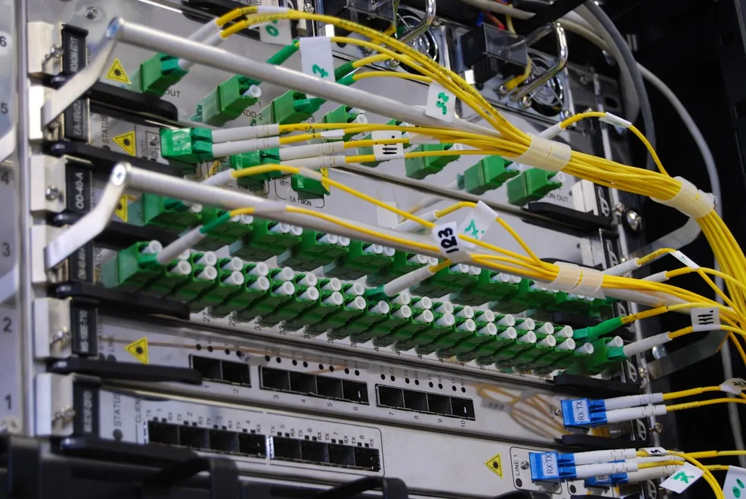
Silicon photonics transmits data between chips using light (photons) instead of electrical signals carried through copper wiring. Copper degrades over distance — signals weaken, heat accumulates, and power consumption climbs. Optical signals bypass these physical constraints entirely, maintaining signal integrity over distances that would cripple copper.
The technology’s leading edge is Co-Packaged Optics (CPO), a design approach that integrates networking chips and optical transceivers into a single package. By shrinking the distance data must travel, CPO slashes both power consumption and latency in one stroke.
The numbers already reflect the shift. Shipments of 800G-and-above transceivers are projected to leap from 24 million units in 2025 to 63 million in 2026 — a 2.6x increase in a single year. That is not gradual adoption; it is a market inflection.
What is driving this acceleration is the economics of AI training at scale. When a cluster needs thousands of GPUs working in lockstep, every watt spent on signal conversion and every microsecond lost to copper-induced latency compounds into measurable cost. CPO eliminates both friction points by putting optical transceivers directly on the chip package.
The New AI Bottleneck: It’s the Wires, Not the Chips
GPU performance doubles with each generation, but the interconnect bandwidth linking those chips together has not kept pace. Nvidia’s NVSwitch delivers 7.2 TB/s of bandwidth. Marvell’s Structera S 60260, with 260 PCIe lanes, tops out at roughly 2.1 TB/s — less than a third of that figure.
Why this matters: as AI models grow larger, no single GPU can handle the workload alone. Hundreds or thousands of GPUs must exchange data simultaneously, and copper wiring becomes the chokepoint. The processors are fast enough; the plumbing is not.
Nvidia’s projected revenue for fiscal year 2027 sits between $150 billion and $160 billion. At that scale, incremental GPU speed improvements yield diminishing returns — but widening the data pipes between those GPUs unlocks entirely new cluster configurations. That insight is the strategic logic behind the $2 billion Marvell investment.
Put simply, the performance ceiling in AI clusters has migrated from the processor to the wire. Nvidia’s bet is that whoever controls the interconnect layer controls the next decade of AI infrastructure economics.
Marvell’s $3.8 Billion Acquisition Spree
Marvell did not become Nvidia’s sole NVLink Fusion partner by accident. In December 2025, Marvell acquired Celestial AI for $3.25 billion, securing the photonic fabric technology that underpins next-generation optical chip-to-chip communication. It was the single largest acquisition in the silicon photonics space.
One month later, in January 2026, Marvell followed up with the $540 million acquisition of XConn Technologies, a firm specializing in AI connectivity solutions. In the span of five months, Marvell deployed $3.8 billion on two acquisitions that pushed its optical DSP (digital signal processing — the semiconductor that converts optical signals to electrical and back) and photonics capabilities to the top of the industry.
In other words, when Nvidia surveyed the field for a partner capable of delivering the scale-up networking that NVLink Fusion demands, Marvell was the only company with the complete technology stack. This was not a conventional equity investment — it was closer to a technology exclusivity play that locks in Marvell’s photonic and interconnect IP for Nvidia’s next-generation architecture.
The timing of Marvell’s acquisition spree suggests these moves were coordinated with the Nvidia partnership well before the public announcement. Celestial AI’s photonic fabric and XConn’s interconnect IP together form the exact combination NVLink Fusion requires to function at the speeds Nvidia is targeting.
$25B Terafab: Musk’s Zero-Experience Bet Against TSMC
UALink vs NVLink: The Interconnect Standards War
Two rival camps are now locked in a direct confrontation over who controls AI data center interconnects. On one side stands UALink, the open standard led by Broadcom and Intel. On the other, Nvidia’s NVLink Fusion ecosystem, freshly expanded by $2 billion in Marvell investment.
Nvidia’s interconnect strategy extends well beyond Marvell. The company has also invested $2 billion each in Lumentum and Coherent, two optical component manufacturers critical to the silicon photonics supply chain. That brings Nvidia’s total investment in photonics infrastructure to $6 billion — a vertical integration play spanning CPO components to chip-level connections.
The takeaway: hyperscalers are hedging. AWS’s next-generation Trainium 4 XPU supports both UALink and NVLink simultaneously, a clear signal that major cloud operators refuse to be locked into a single standard. Yet Nvidia has already deployed $6 billion to pull partners deep into its ecosystem before the standards war reaches a tipping point.
The outcome of this standards battle will reshape AI data center cost structures. If NVLink Fusion becomes the de facto standard, Nvidia’s ecosystem dominance extends from GPUs into the interconnect layer. If UALink prevails, chip designers gain more freedom — but at the cost of integrated performance that closed ecosystems deliver.
For investors, the signal is clear: the interconnect layer is no longer a commodity. It has become strategic terrain, and the companies that control the standards — whether through open coalitions or proprietary ecosystems backed by billions in capital — will extract significant value from every AI cluster built in the coming decade.
$122B OpenAI Funding: The Biggest Private Bet in History
A $17.8 Billion Market: What Investors Should Watch
The global silicon photonics market is projected to grow from $1.8 billion in 2025 to $17.8 billion by 2035, a compound annual growth rate of 25.3%. In 2026 alone, the market is expected to reach $2.3 billion — a 28% expansion in a single year. Wells Fargo estimates the total addressable market for photonics could reach $10 billion to $12 billion by 2030.
The larger opportunity lies in what the industry calls Semi-custom Inference Factories — purpose-built data centers designed for enterprise-specific AI inference workloads. This market is projected to grow into a multi-hundred-billion-dollar opportunity by the end of the decade. NVLink Fusion is the platform Nvidia is building to capture a structural share of that expansion, by becoming the default interconnect standard for every custom inference cluster.
Wells Fargo’s $10 to $12 billion TAM estimate covers the period through 2030. Beyond that horizon, as CPO transitions from premium feature to baseline infrastructure, the interconnect market itself could rival the current GPU market in scale.
Nvidia’s $2 billion is not a bet on Marvell’s stock price. It is a bet on the next decade of AI infrastructure. Two indicators will determine how fast the age of light arrives: the year-over-year growth rate in 800G+ transceiver shipments and the timeline for NVLink Fusion’s first reference design release.
References
- Bloomberg (2026-03-31) — Nvidia announces $2 billion strategic equity investment in Marvell Technology
- FinancialContent (2026-04-01) — NVLink Fusion platform bandwidth of 1.8 TB/s, compatible with Rubin GPUs and Vera CPUs
- 247 Wall St (2026-04-01) — Marvell stock surges 11%, breaks above $106
- NextPlatform (2026-03-31) — Marvell’s $3.25 billion Celestial AI acquisition and $540 million XConn Technologies acquisition
- NextPlatform (2026-03-31) — NVSwitch 7.2 TB/s bandwidth, Structera S 60260 at 2.1 TB/s, Nvidia FY2027 revenue forecast $150-160B
- NextPlatform (2026-03-31) — $2 billion each in Lumentum and Coherent investments, AWS Trainium 4 supporting both UALink and NVLink
- GM Insights (2026) — Global silicon photonics market from $1.8B (2025) to $17.8B (2035), CAGR 25.3%
- FinancialContent (2026-01-01) — 800G+ transceiver shipments from 24 million to 63 million units (2.6x increase)
- ExoSwan (2026) — Wells Fargo estimates photonics TAM at $10-12 billion by 2030
- FinancialContent (2026-04-01) — Semi-custom Inference Factory projected as multi-hundred-billion-dollar market
Stay Ahead of the Curve
Get the latest insights on AI, tech, and markets — delivered in both Korean and English.

Jugger | Backend Developer
A backend engineer working in enterprise solutions software since June 2021. The hands-on perspective from system design, API implementation, and production operations directly informs this site’s
AI, IT, and cloud infrastructure coverage.
For topics outside direct professional experience—blockchain and macroeconomics—analysis is built on primary-source citations such as SEC filings, whitepapers, institutional research, and government
statistics. Speculation is clearly separated from verified fact, and unverified claims are not published.
AI tools assist with drafting, but every article is reviewed, revised, and verified before publication. Errors are corrected with visible notes when discovered.
Contact: jjunggulee@gmail.com